Robust Strain Mapping at Subnanometer Resolution & Subpicometer Precision
Research Theme
Beam Acceleration
Published December 22, 2020
Four-dimensional scanning transmission electron microscopy (4D-STEM) technique along with an electron microscope pixelated array detector (EMPAD) enables spatially resolved mapping of crystal structure with length scales ranging from sub-Angstrom to over micrometers. 4D-STEM works by recording full electron diffraction patterns at each probe position in real-space, which offers a unique opportunity to extract quantitative structural information such as strain, electric and magnetic fields at sub-nm resolution. However, dynamical diffraction effects and specimen mistilts impose challenges for measuring the shifts in Bragg reflections for strain analysis. Here, we present the EWPC (exit-wave power cepstrum) transform approach for robust strain mapping at sub-nm resolution and sub-pm precision. Inspired by cepstral analysis in audio signal processing, EWPC decouples the strain information from crystal mistilts and thickness variation artefacts. It provides a mapping to a good basis for performing machine learning of structure-property relationships, without being dominated by imaging artifacts that have plagued previous approaches.
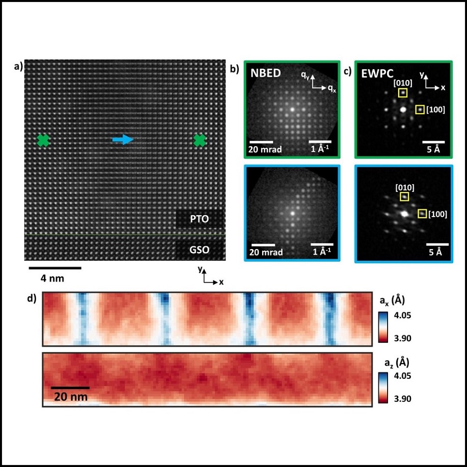
Figure 1: Mapping the lattice parameter of on and off-axis regions of PbTiO₃that occur in ferroelectric domain configurations of PbTiO₃/GdScO₃ (PTO/GSO). a) Atomic resolution STEM shows that at the domain the crystal tilts off-axis and atomic resolution is lost. b) Electron nano diffraction and c) EWPC patterns from the regions of the crystal corresponding to ones like those marked in figure a. a). Electron nanodiffraction shows a clear tilting off-axis but the EWPC spots remain clear. d) EWPC is still able to map the in-plane (ax) and out-of-plane (ay) lattice parameters.
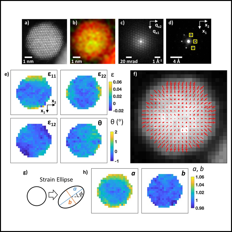
Figure 2: Strain mapping of a core-shell Pt-Co fuel cell catalyst nanoparticle. (a) Atomic resolution STEM image of the particle oriented on the [110] zone axis. (b) EELS composition map showing Pt in red and Co in green. Microprobe STEM conditions were used for NBED mapping of the same particle. (c) Averaged electron nanodiffraction pattern and (d) corresponding EWPC pattern from the center of the particle. EWPC spots circled in red in (d) were used for strain mapping. (e) Maps of strain tensor elements for Lagrange strain referenced to the particle center. (f) Visualization of principal strain vectors as red arrows for both the principal and orthogonal secondary strain directions. (g) Schematic of the strain ellipse construction, with semi-major axis a, semi-minor axis b, and angle of principal strain Φ. (h) Visualizations of the strain ellipse axes a and b.
Reference:
E. Padgett, M. E. Holtz, P. Cueva, Y.-T. Shao, E. Langenberg, D. G. Schlom, and D. A. Muller, “The exit-wave power-cepstrum transform for scanning nanobeam electron diffraction: robust strain mapping at subnanometer resolution and subpicometer precision,” Ultramicroscopy, vol. 214, p. 112994, Jul. 2020, doi: 10.1016/j.ultramic.2020.112994.