
Ultrafast electron diffraction in a keV beamline
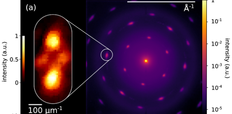
Diffraction pattern produced by a keV electron beam incident on a pair Single hexagonal atomic layers of MoSe2 WSe2 with a relative rotation of XX degrees. The brightest diffraction spots arise from the individual layers, while the small satellites arise from the Moire superstructure. The beam emittance was 0.7 nm-rad.
Like X-rays, a coherent electron beam scattered from a crystalline material forms a diffraction pattern. Such beams can have fs bunch lengths allowing them to probe fast dynamics, and in principle, they can have high transverse coherence, enabling diffraction from crystals with large unit cells. Much previous work in UED has rightly focused on generating short bunch lengths for extreme time resolution.
Recently, grad students Cameron Duncan (Cornell), William Li (Cornell) and Matthew Gordon (U Chicago) used a high-performance semiconductor cathode to produce an electron beam for keV ultrafast diffraction. The emphasis here was to reduce the transverse beam size dramatically, to allow the study of small samples that are hard to fabricate as large crystals. After tuning to avoid expansion of the beam from space charge [ref], using optics that correct aberrations up to sextupole order [ref], and passing the beam through a pinhole, the normalized emittance is under a nanometer-rad and has a temporal resolution about 200
femtoseconds.
So far, this beam has produced a diffraction pattern from a twisted bi-layer whose large structure measures 10 nm. Future work will include the study of thin film heterostructures, and to perform ultrafast electron spectroscopy with high energy resolution.
References:
M. Gordon, W. H. Li, M. B. Andorf, A. C. Bartnik, C. J. R. Duncan, M. Kaemingk, C. A. Pennington, I. V. Bazarov, Y.-K. Kim, and J. M. Maxson, "Four-dimensional emittance measurements of ultrafast electron diffraction optics corrected up to sextupole order", Phys. Rev. Accel. Beams 25, 084001 (2022) [Online] Available: https://journals.aps.org/prab/abstract/10.1103/PhysRevAccelBeams.25.084001
W. H. Li, C.J.R. Duncan, M. B. Andorf, A. C. Bartnik, E. Bianco, L. Cultrera, A. Galdi, M. Gordon, M. Kaemingk, C. A. Pennington, L. F. Kourkoutis, I. V. Bazarov, and J. M. Maxson, "A kiloelectron-volt ultrafast electron micro-diffraction apparatus using low emittance semiconductor photocathodes", Structural Dynamics 9, 024302 (2022) [Online] Available: https://aca.scitation.org/doi/10.1063/4.0000138